Research News
Mar 19, 2026
- Engineering
Lead-free thin films turn everyday vibrations into electricity
Strain-engineered piezoelectric films deliver record performance on silicon
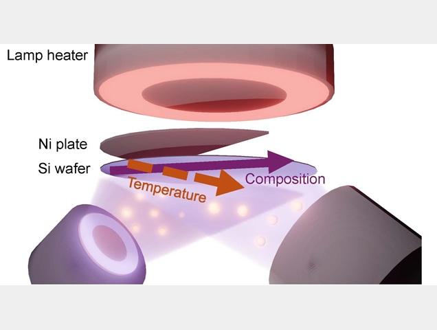
Fabricating lead-free piezoelectric films on silicon
Using a sputtering technique widely employed in semiconductor manufacturing, researchers developed high-quality, lead-free piezoelectric single-crystal thin films directly on standard silicon wafers.
Credit: Osaka Metropolitan University
Powerful electronics don’t have to come at an environmental cost.
Scientists at Osaka Metropolitan University have developed high-performance, lead-free piezoelectric thin films directly on standard silicon wafers. Their results mark a significant step toward production of environmentally friendly energy-harvesting devices that are compatible with conventional semiconductor manufacturing.
Piezoelectric materials generate electric charge from mechanical stress and deform when exposed to an electric field. These materials are common, present for example in microphones, speakers, and headphones, where they convert the vibrations created by music into sound waves.
“We have been working on developing vibration-powered devices as a new application for piezoelectric materials,” said Takeshi Yoshimura, associate professor at Osaka Metropolitan University’s Graduate School of Engineering, and lead author of this study.
“Although piezoelectric materials are already everywhere around us, the highest-performing ones still rely on lead, which is bad for the environment,” he added.
A more environmentally friendly option is bismuth ferrite; its practical use, however, has been limited by high electrical leakage and relatively low efficiency in converting mechanical energy into electrical energy–a process known as piezoelectric performance.
Looking for a lead-free yet still highly efficient alternative, the team engineered a manganese-doped bismuth ferrite ultrathin film grown directly on silicon wafers.
Developing such a device wasn’t easy. Bismuth ferrite doesn’t naturally work on silicon. Compressive strain enhances the piezoelectric properties of bismuth ferrite; however, the silicon wafers, which are required for device fabrication, create the opposite effect, pulling the film during cooling, instead of compressing it.
“Rather than trying to avoid tensile strain, we tried to use it to our advantage,” Yoshimura said. “Our goal was to trigger a structural phase transition that could dramatically improve piezoelectric performance, even on standard silicon wafers.”
Achieving this required overcoming several technical hurdles: the team needed to grow high-quality, single-crystal thin films using sputtering, a deposition technique widely used in the semiconductor industry, while precisely controlling growth temperature. This was particularly difficult because bismuth has a low melting point, making the film composition sensitive to temperature changes.
“We developed a unique ‘biaxial combinatorial sputtering’ technique that allows growth temperature and composition to vary continuously across a single wafer,” Yoshimura said. “This approach enabled dozens of growth conditions to be tested simultaneously, dramatically accelerating optimization compared with conventional trial-and-error methods.”
Using this strategy, the team identified the optimal conditions under which tensile strain induces a structural transition from a rhombohedral to a monoclinic crystal phase, changing its atomic structure into a form that performs better in electronic and energy-harvesting devices. The resulting films achieved the highest piezoelectric response ever reported for this material, suggesting that it would be able to generate a large electric charge.
To test their discovery, the team used vibration energy harvesters, devices that convert mechanical vibrations into electrical energy. When integrated into microelectromechanical systems vibration energy harvesters, the devices showed a fivefold improvement in energy conversion efficiency compared with previous versions, and they operated effectively under both continuous and sudden vibrations, making them suitable for real environments like motors or in devices that are exposed to machine impacts.
Because the films are fabricated entirely by sputtering on standard silicon wafers, the approach is well suited for large-scale manufacturing.
“We aim to expand applications to smart sensors, Internet-of-Things devices, and self-powered devices,” Yoshimura said. “The practical adoption of lead-free piezoelectric materials could contribute to reducing the detrimental environmental impact of future electronics.”
Funding
- Japan Science and Technology Agency as part of Core Research for Evolutional Science and Technology (CREST), grant No. JPMJCR20Q2)
- Adopting Sustainable Partnerships for Innovative Research Ecosystem (ASPIRE), grant No. JPMJAP2312
Paper information
Journal: Microsystems & Nanoengineering
Title: Enhanced Electromechanical Coupling in Piezoelectric MEMS Vibration Energy Harvesters via Strain-induced Phase Transition in Mn-doped Bismuth Ferrite Epitaxial Films
DOI: 10.1038/s41378-026-01177-5
Authors: Sengsavang Aphayvong, Meika Takagi, Kira Fujihara, Yohane Fujibayashi, Norifumi Fujimura, Hidemasa Yamane, Shuichi Murakami, Takeshi Yoshimura
Published: 17 March 2026
URL: https://doi.org/10.1038/s41378-026-01177-5
Contact
Takeshi Yoshimura
Graduate School of Engineering
Email: yoshimura[at]omu.ac.jp
*Please change [at] to @.
SDGs
