Research News
Dec 21, 2023
- Engineering
Are diamonds GaN’s best friend? Revolutionizing transistor technology
Fabrication of a gallium nitride transistor using a diamond substrate that has twice the heat dissipation properties in comparison to silicon carbide.
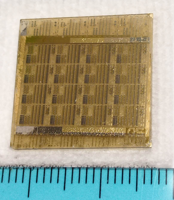
Gallium nitride (GaN) transistor on a diamond substrate
The integration of a 3C-SiC layer between GaN and diamond significantly reduces thermal resistance at the interface and improves heat dissipation, allowing for better performance.
Credit: Jianbo Liang, Osaka Metropolitan University
Researchers at Osaka Metropolitan University are proving that diamonds are so much more than just a girl’s best friend. Their groundbreaking research focuses on gallium nitride (GaN) transistors, which are high-power, high-frequency semiconductor devices used in mobile data and satellite communication systems. With the increasing miniaturization of semiconductor devices, problems arise such as increases in power density and heat generation that can affect the performance, reliability, and lifetime of these devices. Therefore, effective thermal management is crucial. Diamond, which has the highest thermal conductivity of all natural materials, is an ideal substrate material but has not yet been put to practical use due to the difficulties of bonding diamond to GaN elements.
A research team led by Associate Professor Jianbo Liang and Professor Naoteru Shigekawa of the Graduate School of Engineering at Osaka Metropolitan University has successfully fabricated GaN High Electron Mobility Transistors using diamond as a substrate. This novel technology has more than twice the heat dissipation performance of transistors of the same shape fabricated on a silicon carbide (SiC) substrate. To maximize the high thermal conductivity of diamond, the researchers integrated a 3C-SiC layer, a cubic polytype of silicon carbide, between GaN and diamond. This technique significantly reduces the thermal resistance of the interface and improves heat dissipation.
“This new technology has the potential to significantly reduce CO2 emissions and potentially revolutionize the development of power and radio frequency electronics with improved thermal management capabilities,” said Professor Liang.
The results of this research were published in Small.
Funding
This work was based on results obtained from a project, JPNP20004, subsidized by the New Energy and Industrial Technology Development Organization (NEDO). The TEM samples were fabricated at The Oarai Center and the Laboratory of Alpha-Ray Emitters in IMR under the Inter-University Cooperative Research in IMR of Tohoku University (202112-IRKMA-0016). The observation of the TEM samples was supported by Kyoto University Nano Technology Hub in the “Nanotechnology Platform Project” sponsored by the Ministry of Education, Culture, Sports, Science and Technology (MEXT), Japan (JPMXP09A21KT0006). This study was also financially supported by The Fundamental Research Funds for the Central Universities, Peking University.
Paper Information
Journal: Small
Title: High Thermal Stability and Low Thermal Resistance of Large Area GaN/3C-SiC/Diamond Junctions for Practical Device Processes
DOI: 10.1002/smll.202305574
Author: Ryo Kagawa, Zhe Cheng, Keisuke Kawamura, Yutaka Ohno, Chiharu Moriyama, Yoshiki Sakaida, Sumito Ouchi, Hiroki Uratani, Koji Inoue, Yasuyoshi Nagai, Naoteru Shigekawa, and Jianbo Liang
Published: November 14, 2023
URL: https://doi.org/10.1002/smll.202305574
Contact
Graduate School of Engineering
Jianbo Liang
E-mail: liang[at]omu.ac.jp
*Please change [at] to @.
SDGs


